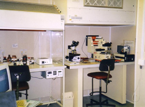
Group Facilities
Class 1000 clean Room with extensive Lithography facilities
It is essential for micron and sub micron work that the patterning of samples is carried out in a clean environment. Even a particle of less than a micron in diameter can be detrimental to sample production. A clean room minimizes the number of dust particles in the atmosphere by an air conditioning system and laminar flow hoods under which the work is carried out. The class of a clean room is determined by the remaining number of dust particles after filtration. The device physics custom built clean room contains equipment used for photolithography and ion beam milling. The photolithography tools used include a programmable variable speed resist spinner, a Karl Suss mask aligner and a developing and wet-etch area.
The device physics cleanroom lithography facilities
Argon Ion Beam milling
Wet etching can often be damaging to samples, and for some materials there are no appropriate chemicals. In these cases Ion Beam milling can be used, which produces a cleaner etch profile and is more controllable and less damaging to delicate samples. The group possess a Millatron IV Argon Ion beam milling machine, a picture of which is shown below:
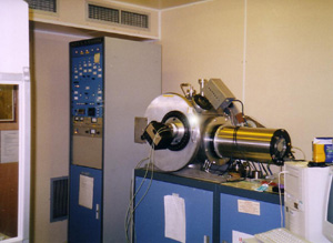
The Ion Beam Milling system 'Milltron IV'
RIE Etching
Reactive Ion Etching (RIE) uses oxygen as the active species to clean and etch samples. We own an automated PLASMALAB RIE Plasma etching system.
In-situ multilayer Magnetron Sputter deposition chamber
The Sputtering system can deposit 2 different materials in-situ. The system is currently set up to deposit thin films of Gold and Niobium, two materials in common use in our devices. The sputtering system has the advantage of being quick and easy to operate, with depositions possible within a couple of hours.
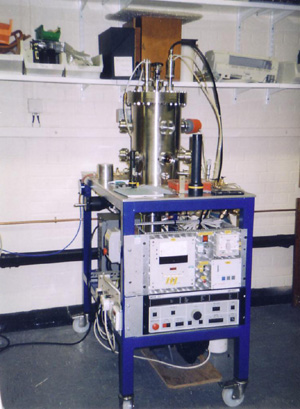
The custom built sputter deposition system
Ultra Low Temperature experimental apparatus
A large amount of experimental apparatus is available to measure fabricated devices. The apparatus is designed to accomodate as many variables as possible so that the devices can be investigated in a number of different ways. For High Tc superconductors, masurements are generally made above 4.2K and therefore Liquid Helium cryostat apparatus is used. For lower Tc superconductors, dilution fridges are available, which can lower the temperature down to 10's of mK. Apparatus contains electrical feedthroughs for the determination of IV characteristics, and multi-axis magnet set-up for investigation into field dependence of samples.
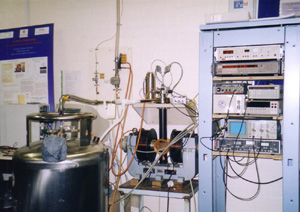
A typical device measurement cryostat setup
SQUID Magnetometer
The SQUID magnetometer is used to make accurate measurements of magnetic field, and can be used to 'image' a magnetic sample. This technique is extremely useful when combining superconducitng materials with ferromagnetic or magneto-resistive materials, as the physics of the interaction between the materials can be established.
Thin Film Laser Ablation facility
Laser ablation is one of the primary methods of thin film deposition used for High Temperature superconducting materials. The group has access to an excimer laser, allowing us to deposit thin films of many materials, including YBCO, STO, LCMO, LSMO, PBCCO. The film growth methods and quality are intensively studied by members of the condensed matter group, resulting in high quality films for use in our device production. To learn more about the laser ablation facility visit the Pulsed Laser deposition website.
Focused Ion Beam Milling apparatus with integrated SEM
The FIB has been one of the most useful tools in recent research. Under vacuum, an energetic beam of Gallium ions is focussed upon the sample, removing material in its path. Very small, precisely milled structures can be acheived down to dimensions of below 100nm. The dual beam system also contains an SEM for high quality imaging of the structures during fabrication. An additional gas assisted deposition system present on the chamber allows structures to be built upon the surface in addition to the milling away of material.
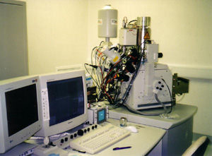
The Dual FIB SEM system
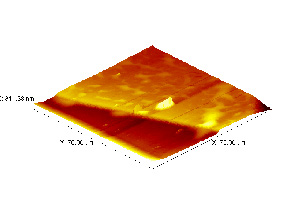
Veeco AFM/STM imaging/lithography system
This new AFM has been recently purchased by the group, replacing the old system. The AFM is principally used for imaging the surfaces of films grown in the laser deposition system, although it is also used to image samples made by the device physcis group. The AFM is of use when accurate measurements of device geometries are required, especially in the z (depth) direction. It is difficult to judge the depth of a milled structure by SEM observation, but the stylus operating principle of the AFM accurately traces out the contours of the sample in 3D. The AFM also has Scanning Tunneling microscopy (STM), Magnetic Force microscopy (MFM) and hi-voltage lithography modes.